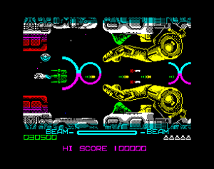
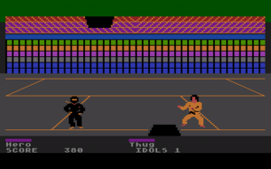
Sometimes we think that we know a lot of how computers work because we know how to code for them at a very low level – directly to the chips registers – we imagine our code almost driving every pixel on the screen, but digging into how to make the display work prove me that I was far from knowing how complex things may turn, even in “simple”computers like the ZX Spectrum.
It was all about timing
Programmers think of the screen as an array of bytes and the video display circuitry as the interpretation of these bytes into a video signal. Pretty good abstraction I must say. It works really well to hide he horrible truth of what is needed to be done, and keep our minds sane.
Chip designers of the early eighties had to work around hard physical restrictions of the time, things that we give for granted today. After reading still half of the book The ZX Spectrum ULA: How to Design a Computer and researching about how the ANTIC/GTIA duo worked on the Atari I can see that the guys who designed those chips were really pushing the envelope, achieving things that were just impossible with the technology available at that time.
And yes, the word time appears every where, the memory access time, the DRAM refresh time, the time required for processing the display memory and the time required to properly drive the CRT tube to create an image on the screen. Yes, it was all about timing… and money. To have a working computer that can properly handle video and still do some stuff, with a price that people could afford, was really challenging.
Clever design
The hardware available was just not that fast, so the designers needed to find ways to make it work faster than the time required to draw a pixel on the screen, and doing it with predictable intervals or the image would be just a dance of unstable pixels. Not only the RAM access was slow, to make it cost effectively they had to use DRAM which is a kind of memory that must be refreshed constantly, so part of the bus access was not to write or read a value on memory, but only to refresh the memory so the content would not be lost.
But that’s half of the problem. The bus access was shared between the CPU and the video chip that needed to read the video memory to process it and display it. Even with the content already read into the chip, the memory was too slow to read the next byte, so they needed to design some kind of parallel processing so the memory could be read at the same time it was processed inside without missing any pixel.
Because if these time restrictions, computers like the Atari 800 and the ZX Spectrum were mostly video driven. They were built around the TV standards of the time: NTSC and PAL. The clock signal that drove all the system was calculated to create the display for each one of those TV standards. Let’s look a bit deeper.
ZX Spectrum video display generation
A simple design decision shows how video driven this computer was: The ULA – that was the chip that drives the video – is the system controller at the point that the clock signal used by the CPU was sent by this chip. This allowed the ULA to synchronize the access to the bus halting the CPU until the access was finished, and the CPU never knew that it happened. Every time the ULA required access to the display memory, or needed to refresh the DRAM, the clock signal to the CPU was stopped and thus the CPU halted. The ULA had the priority.
The way the screen data was interpreted gives this computer an unique aesthetics: The colors where arranged in a way that each block of 8×8 pixels required only 9 bytes, 8 for the bitmap and 1 for the colors used on it. So a screen of 256×192 with 15 colors required only 6912 bytes, and that resolution was considered high for that range of computers. Also the video memory was arranged in a way that the bytes where the pixels and attributes were stored were read from similar locations (locality principle) and so the DRAM was refreshed at the same time. One can see that design when loading a screen from tape, the lines are not read in sequence, and the attributes are at the end of the content being read.

Having this architecture imposed some trade offs: Having a high color resolution would have required more system memory and so less available for programs, also reading more memory would have slowed down the processor because it would have needed to be halted more frequently. So they needed to find way to have a high resolution with the less memory requirements, and they achieved it. The original designers thought that text screens would have plenty of colors with this design and this was needed for a good personal computer, but they didn’t think about games. Surprisingly, the computer turned out to be so popular and quite fast because of this design that a lot of games got ported into it. To me at least, it is always interesting to see how game programmers worked around the color limitations on this machine.
As a side note, the ULA name was not specific to the video chip found in this computer, it was the name of the technology being used on it. An ULA was a chip with no logic on it, it was just a “logic array” with non-commited logic. It was open to any logic design, hence the letter “U” for “Uncommited”. The logic was applied at the last stages of production as a layer that connected the logic units to implement a particular logic design. It was cheap, flexible and it supported evolving development of the hardware design. Sound familiar? Yes, it was like an early kind of FPGA.
Atari 800 video generation
This is a whole line of computer where you can also find the XL and XE variants (800XL, 65XE, 13oXE and probably others). The video display design in these computers is a departure from the experience they already have in the Atari 2600 design, where the CPU renders each scan line as it is drawn on the screen, limiting the resolution and also the CPU time required to do the logic part. Not to think about how complex was to make something different from Pong with that hardware.
With the Atari 800 they splitted the video signal generation in two chips: The Antic processor was responsable of reading the video memory and converting it into a bit stream that was fed into a second processor, the GTIA. The GTIA just made a color interpretation of the bit stream, added overlaid “sprites” (player/missiles) and created the final video signal.
Again, the computer was built around the video timings. For every two pixels on the screen there was one CPU cycle. The system was ran by a clock at a speed required to draw the pixels on the screen, also known as “pixel clock”, and that clock was halved to drive the CPU. For example, on NTSC regions the main clock was ran at 3.58Mhz and the clock fed to the CPU was at 3.58 / 2 = 1.79Mhz. Not surprisingly, other systems on the same region clocked their Z80 CPU’s at the full speed of 3.58Mhz.
Now this is funny… I’m from the old school Linux users that had to mess with the “modelines” when setting up some VGA modes. Part of the modeline math was calculating the pixel clock speed, which is this same frequency that we are talking about here. More about this in a future post.

Back to the Atari, again the video display had the priority, the CPU was halted when it required access to read the memory. This also helped add a really cool feature, the CPU can be halted until a scanline is drawn just writing to a specific Antic register (WSYNC). This allows safely changing some display registers at any horizontal position of the screen, like changing colors or repositioning the sprites to have more than it was possible for a single screen.
The chip designers were later involved in another marvel of that age, the Amiga Computer. And they didn’t stop there, one of the designers was later involved in the design of USB and Bluetooth among other stuff.
If you are still reading, this post was meant only an introduction that will help understand the preliminar design of the video chip for Compy in this next post.