This post is part of a series of three post about the recent updates on the FPGA implementation of Compy.
- Compy FPGA – Palettes and line buffers
- Compy FPGA – VRAM and Cornet CPU
- Compy FPGAs and how I got here (this one)
I had a lot of problems in the way. A lot! Fortunately they are part of the past now and I finally started to walk instead of crawl. Following are some of those stones that I hit in the road.
Which FPGA to use for development
When I started I didn’t have a clue of what FPGA I would need, so I decided to start with something cheap with enough connections to not miss anything. If that board would fell short I would know better which one I would need, and in fact, that was what happened.
I think that I started with the right foot choosing an Altera FPGA, I just can develop everything on Linux and there is more than enough, I mean, a lot more than enough documentation for my needs. The development environment is simple and on the long run it starts to feel familiar. Some tools like the Signal Tap Analyzer ended to be critical, but more on that later.
My first FPGA was a development board with a Cyclone IV with 6KLE. I got it for around USD$70 at that time. It fell short mainly for two reasons: I started using 40% of its capacity as early I started going beyond the basics, and the amount of block ram available (32K+) forced me to depend on the SRAM for everything. In the middle I got the Arrow SoCKit which is a beast, it has 110KLE, 2GB of DDR3 RAM, even an ARM CPU and I got it for USD$60.
The SoCKit has two main problems: One is that the RAM is harder to use and you also need to interact with the ARM CPU. The other problem which was a blocker for me is that the price that I got for it was not real, it can be easily go beyond USD$300 and I think I shouldn’t design for a device that most people would find expensive and overpowered like I find it now.
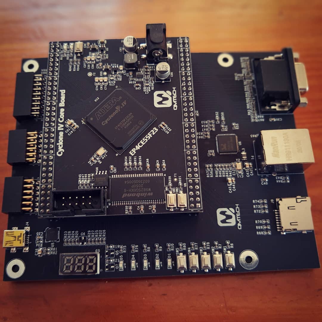
Fortunately I was able to find a middle spot, which is a Cyclone IV with 55KLE. These are the parts that I like the most:
- The price for a development kit is around USD$80, almost the same price that I started with
- You can get it as a core board + a daughter board with sdcard, port, buttons etc. For the future it should be easy to create a custom board for Compy just adding the same core board provided for less than $60 (for the core board)
- It has plenty of block ram (256K+) which allowed me to use it for the video RAM as described earlier.
Timing is critical
The main problem that I had was with timings. I read a lot about it but even being aware of the existence of the problem I didn’t realize that I was just having that problem. For a software engineer like me, one has a way of thinking that is very different than a hardware engineer. One comes from a sequential world and the hardware world is mainly parallel, you need to turn your sequential approach and divide it in bits of small parallel tasks. If you don’t get small enough, your logic just can’t be executed in the required clock cycle.
Another problem is that you just cannot use several clocks and share data between them. That’s an area that is very well studied and explained but again, I didn’t realize how critical it was. I was getting builds that ran flawlessly, then then next time the same logic glitched and I didn’t know why.
I would never give enough thanks to Daniel Serpell that helped me to realize of these issues and how there were all around my design. He gave me invaluable pointers to get them fixed and finally move forwards.
Daniel also has his own 6502 based computer, and from time to time I go to read his verilog code to check how he solved the issues that I find often with my design. I also have looked at several MiST cores, they are harder to read but they also help to check how different systems resolved common issues.
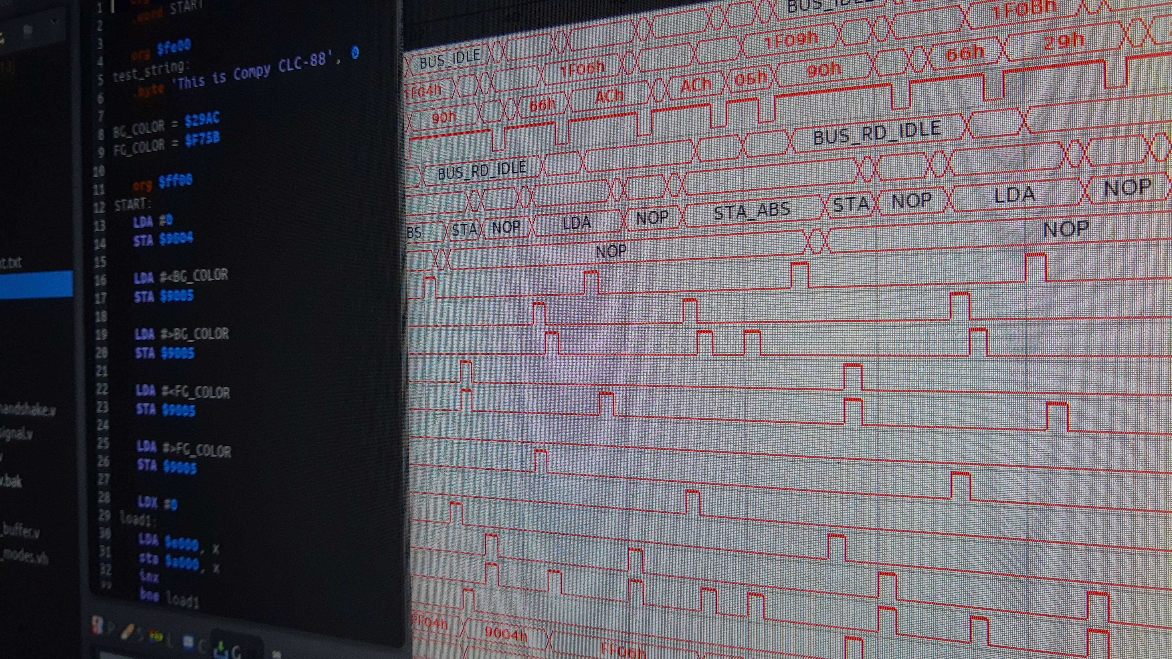
Signal Tap Analyzer
One of the most difficult parts for me was to know what was happening with my design in the FPGA. I did several approaches, like using the amazing 8bitworkshop IDE to simulate some parts of my design, or using the video output to display some events, like using specially colored pixels to display when video RAM was being read. It was some sort of “printf” for hardware design.
I knew that in the past people used oscilloscopes to see what was going on, but for me it was out of my reach. I knew that a tool called Signal Tap would help, but for some reason I wasn’t able to display any signals after several tries. Finally I understood how to set it up and it just changed my whole workflow. Now I know that if I get a behaviour that I don’t understand, I can always use Signal Tap and see the all the signals in all their glory, even keeping all the symbolic names! Again, it was a fortune to select Altera for my FPGA implementation.
Back to the first post of this series: Compy FPGA – Palettes and line buffers